UPSC Current Affairs
Semiconductors
A semiconductoris a material which has an electrical conductivity value falling between that of a conductor, such as copper, and an insulator, such as glass. Its resistivity falls as its temperature rises; metals behave in the opposite way. Its conductingproperties may be altered in useful ways by introducing impurities ("doping") into the crystal structure.
VRAuthor Desk
3 min read
A semiconductoris a material which has an electrical conductivity value falling between that of a conductor, such as copper, and an insulator, such as glass. Its resistivity falls as its temperature rises; metals behave in the opposite way. Its conductingproperties may be altered in useful ways by introducing impurities ("doping") into the crystal structure.
- A semiconductoris a material which has an electrical conductivity value falling between that of a conductor, such as copper, and an insulator, such as glass.
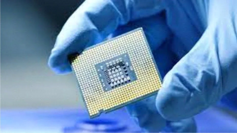
- Its resistivity falls as its temperature rises; metals behave in the opposite way.
- Its conductingproperties may be altered in useful ways by introducing impurities ("doping") into the crystal structure.
- When two differently doped regions exist in the same crystal, a semiconductor junction is created.
- Semiconductor devices can display a range of different useful properties, such as passing current more easily in one direction than the other, showing variable resistance, and having sensitivity to light or heat.
- Because the electrical properties of a semiconductor material can be modified by doping and by the application of electrical fields or light, devices made from semiconductors can be used for amplification, switching, and energy conversion.
- Doping greatly increases the number of charge carriers within the crystal.
- When a doped semiconductor contains free holes, it is called "p-type", and when it contains free electrons, it is known as "n-type".
- The semiconductor materials used in electronic devices are doped under precise conditions to control the concentration and regions of p- and n-type dopants.
- A single semiconductor device crystal can have many p- and n-type regions; the p–n junctions between these regions are responsible for the useful electronic behavior.
- Using a hot-point probe, one can determine quickly whether a semiconductor sample is p- or n-type.
India semiconductor mission:
- India Semiconductor Mission (ISM) is a specialized and independent Business Division within the Digital India Corporation that aims to build a vibrant semiconductor and display ecosystem to enable India’s emergence as a global hub for electronics manufacturing and design.
ISM has been proposed with the objective to:
- Formulate a comprehensive long-term strategy for developing sustainable semiconductors and display manufacturing facilities and semiconductor design eco-system in the country in consultation with the Government ministries/departments/agencies, industry, and academia.
- Facilitate the adoption of secure microelectronics and developing a trusted semiconductor supply chain, including raw materials, specialty chemicals, gases, and manufacturing equipment.
- Enable a multi-fold growth of the Indian semiconductor design industry by providing requisite support in the form of Electronic Design Automation (EDA) tools, foundry services and other suitable mechanisms for early-stage startups.
- Promote and facilitate indigenous Intellectual Property (IP) generation.
- Encourage, enable and incentivize Transfer of Technologies (ToT).
- Establish suitable mechanisms to harness economies of scale in Indian semiconductor and display industry.
- Enable cutting-edge research in semiconductors and display industry including evolutionary and revolutionary technologies through grants, global collaborations and other mechanisms in academia/research institutions, industry, and through establishing Centres of Excellence (CoEs).
- Enable collaborations and partnership programs with national and international agencies, industries and institutions for catalyzing collaborative research, commercialization and skill development.
Syllabus: Prelims
- Prelims: Key facts, institutions, locations and terminology in the article.
- Mains: Connect the topic with Economy, Polity & Governance, Science & Technology.
- Revision: Use the article headings to prepare concise notes and answer-writing points.
Test your understanding
Questions from this article
Prelims practiceWith reference to Semiconductors, consider the following statements:
- A semiconductoris a material which has an electrical conductivity value falling between that of a conductor, such as copper, and an insulator, such as glass.
- Its resistivity falls as its temperature rises; metals behave in the opposite way.
- Its conductingproperties may be altered in useful ways by introducing impurities ("doping") into the crystal structure.
Which of the statements given above are correct?
- 1 and 2 only
- 2 and 3 only
- 1 and 3 only
- 1, 2 and 3
View answer
Answer: (d) 1, 2 and 3. All three statements are drawn from the article.
Mains practiceDiscuss the background, key issues and significance of Semiconductors for India.
Answer in 250 words.
View answer approach
- India semiconductor mission:
- ISM has been proposed with the objective to:
- Background and context
- Key facts and institutional framework
- Significance and way forward
Frequently asked questionsFrequently asked questions
Why is Semiconductors in the news?
A semiconductoris a material which has an electrical conductivity value falling between that of a conductor, such as copper, and an insulator, such as glass. Its resistivity falls as its temperature rises; metals behave in the opposite way.
What are the key facts about Semiconductors?
Its conductingproperties may be altered in useful ways by introducing impurities ("doping") into the crystal structure. When two differently doped regions exist in the same crystal, a semiconductor junction is created. Semiconductor devices can display a range of different useful properties, such as passing current more easily in one direction than the other, showing variable resistance, and having sensitivity to light or heat.
Why is Semiconductors important for UPSC preparation?
The topic connects current developments with Economy, Polity & Governance, Science & Technology and is relevant for both objective revision and analytical answer writing.